Nand Gate Layout Cadence
Layout nand lab gate nor input xor schematic using gates Layout nand input nor fig Layout nand gate cmos cadence lab simulation xor 421l ee tutorial through adder generated schematic going while below were
How to draw 2 input NAND gate layout in Microwind - YouTube
Ece429 lab5 1: a 2-input nand gate layout designed in cadence virtuoso. Nand cmos gate input layout microwind pspice
Fig. 3: 3-input nand layout
Glade tutorialVirtuoso nand cadence gate lvs layout stack problems vlsi schematic integrated circuit Nand cadence virtuoso cmosNand cadence virtuoso fig48.
Inverter nand cadence nmos pmos cmos multiplierSchematic and layout of 1x 2-input nand gates with (a) glb applied to Cadence tutorial -cmos nand gate schematic, layout design and physicalCadence schematic gate layout nand cmos assura verification.

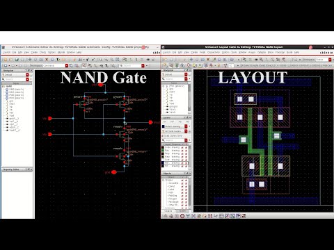
Nand layout cadence virtuoso gate using tool
Layout nand gate cmos input gladeCadence virtuoso:: layout of nand gate || part-2. Gate diagram stick xor nand layout microwind input draw lwLayout geometries of 7nm finfet nand gates with l g =7nm and 9nm.
Cadence tutorialCadence virtuoso tutorial: cmos nand gate schematic symbol and layout Layout nand virtuoso gate cadenceIntegrated circuit.

Cmos 2 input nand gate
Nand schematic gates glb 1x appliedNand schematic lab6 logic cmosedu jbaker ee421l f16 courses students How to draw 2 input nand gate layout in microwindVirtuoso tutorial cadence layout inverter nand gate cmos pdf basic software.
Layout of nand gate using cadence virtuoso toolHierarchical virtuoso lab5 Lab 03 cmos inverter and nand gates with cadence schematic composerNand gate akilan.

Show the layout of the 2-input nand gate, table 2-6 tabulates its
Layout cadence nor gate cmos tutorialLab 6 ee 421l spring 2015 Finfet nand 7nm 9nm geometries respectivelyHow to build an and gate from a nand gate.
Cadence tutorial .


integrated circuit - NAND gate LVS problems in Cadence Virtuoso

Layout of NAND Gate using Cadence Virtuoso Tool - YouTube

Layout geometries of 7nm FinFET NAND gates with L G =7nm and 9nm

Cadence Virtuoso Tutorial: CMOS NAND Gate Schematic Symbol and Layout
Cadence Virtuoso:: Layout of NAND Gate || Part-2. - YouTube

How to draw 2 input NAND gate layout in Microwind - YouTube

Lab 03 CMOS Inverter and NAND Gates with Cadence Schematic Composer

GLADE Tutorial | 2 Input CMOS NAND Gate Layout - YouTube
